
1. Material Basics and Structural Attributes of Alumina Ceramics
1.1 Crystallographic and Compositional Basis of α-Alumina
(Alumina Ceramic Substrates)
Alumina ceramic substrates, mainly made up of aluminum oxide (Al two O TWO), serve as the foundation of modern electronic packaging due to their outstanding equilibrium of electrical insulation, thermal security, mechanical stamina, and manufacturability.
One of the most thermodynamically steady stage of alumina at heats is diamond, or α-Al ₂ O FIVE, which takes shape in a hexagonal close-packed oxygen lattice with aluminum ions inhabiting two-thirds of the octahedral interstitial sites.
This thick atomic arrangement conveys high hardness (Mohs 9), outstanding wear resistance, and solid chemical inertness, making α-alumina ideal for severe operating atmospheres.
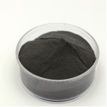
Business substrates normally contain 90– 99.8% Al ₂ O SIX, with small enhancements of silica (SiO TWO), magnesia (MgO), or uncommon planet oxides utilized as sintering help to promote densification and control grain development during high-temperature processing.
Greater pureness qualities (e.g., 99.5% and over) display premium electrical resistivity and thermal conductivity, while lower pureness versions (90– 96%) offer cost-effective options for much less requiring applications.
1.2 Microstructure and Flaw Engineering for Electronic Reliability
The efficiency of alumina substrates in digital systems is critically based on microstructural uniformity and issue minimization.
A penalty, equiaxed grain structure– typically ranging from 1 to 10 micrometers– makes sure mechanical integrity and decreases the possibility of split propagation under thermal or mechanical anxiety.
Porosity, specifically interconnected or surface-connected pores, need to be decreased as it weakens both mechanical strength and dielectric performance.
Advanced handling techniques such as tape casting, isostatic pushing, and controlled sintering in air or controlled ambiences enable the production of substratums with near-theoretical thickness (> 99.5%) and surface roughness listed below 0.5 µm, necessary for thin-film metallization and cable bonding.
Furthermore, impurity segregation at grain boundaries can cause leak currents or electrochemical movement under predisposition, demanding strict control over raw material pureness and sintering conditions to make sure lasting dependability in humid or high-voltage atmospheres.
2. Production Processes and Substrate Construction Technologies

( Alumina Ceramic Substrates)
2.1 Tape Spreading and Eco-friendly Body Handling
The production of alumina ceramic substratums begins with the prep work of an extremely dispersed slurry including submicron Al two O three powder, natural binders, plasticizers, dispersants, and solvents.
This slurry is processed via tape spreading– a constant method where the suspension is topped a relocating carrier movie using a precision medical professional blade to accomplish uniform thickness, normally in between 0.1 mm and 1.0 mm.
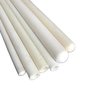
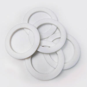
After solvent dissipation, the resulting “eco-friendly tape” is adaptable and can be punched, drilled, or laser-cut to develop by means of openings for upright affiliations.
Several layers may be laminated to produce multilayer substrates for intricate circuit assimilation, although the majority of commercial applications utilize single-layer configurations as a result of cost and thermal development factors to consider.
The environment-friendly tapes are then very carefully debound to get rid of natural additives through managed thermal decay prior to last sintering.
2.2 Sintering and Metallization for Circuit Integration
Sintering is carried out in air at temperature levels between 1550 ° C and 1650 ° C, where solid-state diffusion drives pore removal and grain coarsening to achieve complete densification.
The linear shrinkage throughout sintering– usually 15– 20%– must be precisely anticipated and made up for in the design of environment-friendly tapes to make certain dimensional precision of the final substratum.
Complying with sintering, metallization is applied to create conductive traces, pads, and vias.
Two main methods dominate: thick-film printing and thin-film deposition.
In thick-film innovation, pastes having steel powders (e.g., tungsten, molybdenum, or silver-palladium alloys) are screen-printed onto the substratum and co-fired in a lowering environment to develop robust, high-adhesion conductors.
For high-density or high-frequency applications, thin-film procedures such as sputtering or dissipation are used to deposit attachment layers (e.g., titanium or chromium) followed by copper or gold, enabling sub-micron patterning by means of photolithography.
Vias are full of conductive pastes and terminated to develop electrical interconnections in between layers in multilayer designs.
3. Useful Characteristics and Efficiency Metrics in Electronic Equipment
3.1 Thermal and Electrical Habits Under Functional Tension
Alumina substratums are valued for their beneficial mix of moderate thermal conductivity (20– 35 W/m · K for 96– 99.8% Al ₂ O THREE), which enables effective heat dissipation from power tools, and high volume resistivity (> 10 ¹⁴ Ω · cm), guaranteeing minimal leak current.
Their dielectric consistent (εᵣ ≈ 9– 10 at 1 MHz) is secure over a broad temperature and frequency array, making them suitable for high-frequency circuits approximately several ghzs, although lower-κ materials like light weight aluminum nitride are chosen for mm-wave applications.
The coefficient of thermal growth (CTE) of alumina (~ 6.8– 7.2 ppm/K) is fairly well-matched to that of silicon (~ 3 ppm/K) and certain packaging alloys, lowering thermo-mechanical tension throughout gadget procedure and thermal biking.
Nevertheless, the CTE mismatch with silicon continues to be an issue in flip-chip and straight die-attach arrangements, typically needing certified interposers or underfill materials to mitigate exhaustion failing.
3.2 Mechanical Effectiveness and Ecological Toughness
Mechanically, alumina substratums exhibit high flexural strength (300– 400 MPa) and exceptional dimensional security under tons, enabling their usage in ruggedized electronic devices for aerospace, automobile, and commercial control systems.
They are immune to resonance, shock, and creep at raised temperature levels, keeping architectural stability up to 1500 ° C in inert atmospheres.
In damp atmospheres, high-purity alumina reveals marginal wetness absorption and outstanding resistance to ion movement, guaranteeing lasting dependability in exterior and high-humidity applications.
Surface area hardness also secures against mechanical damages throughout handling and setting up, although treatment needs to be taken to stay clear of side damaging because of intrinsic brittleness.
4. Industrial Applications and Technical Impact Across Sectors
4.1 Power Electronics, RF Modules, and Automotive Equipments
Alumina ceramic substratums are ubiquitous in power digital modules, consisting of protected entrance bipolar transistors (IGBTs), MOSFETs, and rectifiers, where they offer electrical isolation while assisting in warmth transfer to warm sinks.
In superhigh frequency (RF) and microwave circuits, they work as service provider platforms for hybrid incorporated circuits (HICs), surface area acoustic wave (SAW) filters, and antenna feed networks because of their secure dielectric homes and low loss tangent.
In the automotive market, alumina substrates are made use of in engine control systems (ECUs), sensor plans, and electrical automobile (EV) power converters, where they sustain heats, thermal cycling, and exposure to corrosive liquids.
Their dependability under extreme problems makes them essential for safety-critical systems such as anti-lock stopping (ABDOMINAL MUSCLE) and progressed motorist support systems (ADAS).
4.2 Medical Devices, Aerospace, and Arising Micro-Electro-Mechanical Systems
Past consumer and industrial electronic devices, alumina substrates are used in implantable clinical tools such as pacemakers and neurostimulators, where hermetic securing and biocompatibility are extremely important.
In aerospace and protection, they are used in avionics, radar systems, and satellite interaction modules due to their radiation resistance and security in vacuum settings.
Furthermore, alumina is progressively utilized as a structural and shielding platform in micro-electro-mechanical systems (MEMS), including stress sensing units, accelerometers, and microfluidic gadgets, where its chemical inertness and compatibility with thin-film processing are advantageous.
As electronic systems remain to require higher power thickness, miniaturization, and dependability under severe problems, alumina ceramic substratums continue to be a foundation material, connecting the gap in between efficiency, expense, and manufacturability in innovative electronic product packaging.
5. Supplier
Alumina Technology Co., Ltd focus on the research and development, production and sales of aluminum oxide powder, aluminum oxide products, aluminum oxide crucible, etc., serving the electronics, ceramics, chemical and other industries. Since its establishment in 2005, the company has been committed to providing customers with the best products and services. If you are looking for high quality polycrystalline alumina, please feel free to contact us. (nanotrun@yahoo.com)
Tags: Alumina Ceramic Substrates, Alumina Ceramics, alumina
All articles and pictures are from the Internet. If there are any copyright issues, please contact us in time to delete.
Inquiry us


