
1. Material Features and Structural Stability
1.1 Intrinsic Characteristics of Silicon Carbide
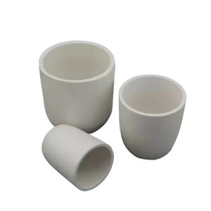
(Silicon Carbide Crucibles)
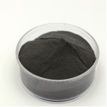
Silicon carbide (SiC) is a covalent ceramic compound made up of silicon and carbon atoms prepared in a tetrahedral lattice structure, mainly existing in over 250 polytypic forms, with 6H, 4H, and 3C being one of the most technically appropriate.
Its strong directional bonding imparts phenomenal solidity (Mohs ~ 9.5), high thermal conductivity (80– 120 W/(m · K )for pure solitary crystals), and outstanding chemical inertness, making it among the most robust materials for extreme atmospheres.
The large bandgap (2.9– 3.3 eV) ensures exceptional electric insulation at area temperature level and high resistance to radiation damages, while its reduced thermal development coefficient (~ 4.0 × 10 ⁻⁶/ K) contributes to premium thermal shock resistance.
These intrinsic residential or commercial properties are preserved even at temperature levels surpassing 1600 ° C, permitting SiC to keep structural stability under extended exposure to molten steels, slags, and reactive gases.
Unlike oxide porcelains such as alumina, SiC does not react readily with carbon or type low-melting eutectics in minimizing ambiences, an essential benefit in metallurgical and semiconductor handling.
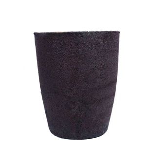
When fabricated right into crucibles– vessels developed to have and warm materials– SiC exceeds conventional products like quartz, graphite, and alumina in both life expectancy and process integrity.
1.2 Microstructure and Mechanical Stability
The performance of SiC crucibles is closely connected to their microstructure, which relies on the production technique and sintering additives utilized.
Refractory-grade crucibles are normally generated using response bonding, where permeable carbon preforms are penetrated with molten silicon, forming β-SiC through the reaction Si(l) + C(s) → SiC(s).
This procedure yields a composite structure of primary SiC with residual complimentary silicon (5– 10%), which improves thermal conductivity but may limit usage over 1414 ° C(the melting factor of silicon).
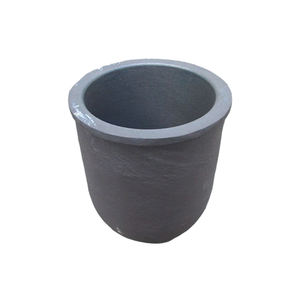
Additionally, completely sintered SiC crucibles are made through solid-state or liquid-phase sintering making use of boron and carbon or alumina-yttria additives, attaining near-theoretical density and greater pureness.
These display superior creep resistance and oxidation stability yet are a lot more costly and tough to fabricate in large sizes.
( Silicon Carbide Crucibles)
The fine-grained, interlacing microstructure of sintered SiC provides excellent resistance to thermal exhaustion and mechanical disintegration, important when managing liquified silicon, germanium, or III-V compounds in crystal development procedures.
Grain border engineering, including the control of second phases and porosity, plays an essential role in figuring out long-term toughness under cyclic heating and hostile chemical settings.
2. Thermal Efficiency and Environmental Resistance
2.1 Thermal Conductivity and Heat Circulation
One of the defining advantages of SiC crucibles is their high thermal conductivity, which makes it possible for quick and uniform warmth transfer throughout high-temperature handling.
In contrast to low-conductivity materials like fused silica (1– 2 W/(m · K)), SiC efficiently distributes thermal power throughout the crucible wall surface, minimizing localized locations and thermal gradients.
This harmony is crucial in procedures such as directional solidification of multicrystalline silicon for photovoltaics, where temperature level homogeneity directly impacts crystal quality and issue thickness.
The combination of high conductivity and reduced thermal expansion causes a remarkably high thermal shock specification (R = k(1 − ν)α/ σ), making SiC crucibles resistant to splitting throughout fast heating or cooling down cycles.
This enables faster furnace ramp prices, enhanced throughput, and reduced downtime because of crucible failure.
Moreover, the product’s capacity to withstand repeated thermal biking without substantial deterioration makes it excellent for batch handling in industrial furnaces operating over 1500 ° C.
2.2 Oxidation and Chemical Compatibility
At elevated temperature levels in air, SiC goes through passive oxidation, creating a protective layer of amorphous silica (SiO TWO) on its surface area: SiC + 3/2 O ₂ → SiO ₂ + CO.
This glazed layer densifies at heats, acting as a diffusion barrier that slows more oxidation and protects the underlying ceramic structure.
Nonetheless, in minimizing atmospheres or vacuum problems– common in semiconductor and metal refining– oxidation is reduced, and SiC continues to be chemically stable versus liquified silicon, aluminum, and several slags.
It resists dissolution and response with molten silicon as much as 1410 ° C, although prolonged exposure can cause minor carbon pick-up or user interface roughening.
Most importantly, SiC does not introduce metallic contaminations into delicate melts, an essential need for electronic-grade silicon production where contamination by Fe, Cu, or Cr has to be maintained listed below ppb degrees.
Nevertheless, treatment should be taken when refining alkaline earth steels or extremely reactive oxides, as some can corrode SiC at severe temperatures.
3. Production Processes and Quality Assurance
3.1 Fabrication Strategies and Dimensional Control
The production of SiC crucibles includes shaping, drying out, and high-temperature sintering or infiltration, with approaches picked based on called for purity, dimension, and application.
Usual creating techniques consist of isostatic pressing, extrusion, and slip spreading, each using various levels of dimensional accuracy and microstructural harmony.
For huge crucibles used in solar ingot casting, isostatic pushing guarantees consistent wall surface thickness and density, decreasing the risk of asymmetric thermal development and failing.
Reaction-bonded SiC (RBSC) crucibles are affordable and commonly utilized in foundries and solar sectors, though recurring silicon restrictions maximum service temperature.
Sintered SiC (SSiC) variations, while more expensive, deal superior purity, strength, and resistance to chemical attack, making them ideal for high-value applications like GaAs or InP crystal growth.
Precision machining after sintering might be called for to achieve tight tolerances, especially for crucibles utilized in upright slope freeze (VGF) or Czochralski (CZ) systems.
Surface area completing is critical to minimize nucleation websites for issues and make sure smooth thaw flow during spreading.
3.2 Quality Control and Efficiency Validation
Rigorous quality control is important to make sure integrity and long life of SiC crucibles under demanding functional problems.
Non-destructive analysis techniques such as ultrasonic screening and X-ray tomography are employed to detect internal splits, gaps, or thickness variations.
Chemical analysis using XRF or ICP-MS validates reduced degrees of metal pollutants, while thermal conductivity and flexural stamina are measured to verify product consistency.
Crucibles are often based on simulated thermal biking tests before delivery to identify possible failure modes.
Set traceability and accreditation are conventional in semiconductor and aerospace supply chains, where part failure can result in expensive production losses.
4. Applications and Technological Influence
4.1 Semiconductor and Photovoltaic Industries
Silicon carbide crucibles play a crucial role in the manufacturing of high-purity silicon for both microelectronics and solar cells.
In directional solidification heaters for multicrystalline solar ingots, huge SiC crucibles act as the primary container for liquified silicon, sustaining temperatures over 1500 ° C for numerous cycles.
Their chemical inertness prevents contamination, while their thermal security makes certain uniform solidification fronts, bring about higher-quality wafers with less dislocations and grain boundaries.
Some manufacturers coat the inner surface area with silicon nitride or silica to further lower adhesion and facilitate ingot launch after cooling down.
In research-scale Czochralski development of substance semiconductors, smaller SiC crucibles are made use of to hold thaws of GaAs, InSb, or CdTe, where marginal sensitivity and dimensional stability are vital.
4.2 Metallurgy, Factory, and Emerging Technologies
Beyond semiconductors, SiC crucibles are vital in metal refining, alloy preparation, and laboratory-scale melting procedures including light weight aluminum, copper, and rare-earth elements.
Their resistance to thermal shock and disintegration makes them suitable for induction and resistance heating systems in foundries, where they last longer than graphite and alumina alternatives by a number of cycles.
In additive production of reactive metals, SiC containers are utilized in vacuum induction melting to avoid crucible malfunction and contamination.
Arising applications consist of molten salt reactors and focused solar power systems, where SiC vessels may consist of high-temperature salts or liquid steels for thermal power storage space.
With continuous advancements in sintering technology and covering engineering, SiC crucibles are positioned to sustain next-generation materials processing, making it possible for cleaner, more effective, and scalable industrial thermal systems.
In recap, silicon carbide crucibles stand for a critical making it possible for technology in high-temperature material synthesis, integrating remarkable thermal, mechanical, and chemical efficiency in a solitary engineered component.
Their extensive adoption throughout semiconductor, solar, and metallurgical sectors emphasizes their duty as a foundation of contemporary industrial porcelains.
5. Vendor
Advanced Ceramics founded on October 17, 2012, is a high-tech enterprise committed to the research and development, production, processing, sales and technical services of ceramic relative materials and products. Our products includes but not limited to Boron Carbide Ceramic Products, Boron Nitride Ceramic Products, Silicon Carbide Ceramic Products, Silicon Nitride Ceramic Products, Zirconium Dioxide Ceramic Products, etc. If you are interested, please feel free to contact us.
Tags: Silicon Carbide Crucibles, Silicon Carbide Ceramic, Silicon Carbide Ceramic Crucibles
All articles and pictures are from the Internet. If there are any copyright issues, please contact us in time to delete.
Inquiry us


