
1. Crystal Structure and Polytypism of Silicon Carbide
1.1 Cubic and Hexagonal Polytypes: From 3C to 6H and Beyond
(Silicon Carbide Ceramics)
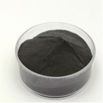
Silicon carbide (SiC) is a covalently adhered ceramic composed of silicon and carbon atoms organized in a tetrahedral control, forming among the most complicated systems of polytypism in products science.
Unlike a lot of porcelains with a single secure crystal framework, SiC exists in over 250 known polytypes– distinct piling series of close-packed Si-C bilayers along the c-axis– ranging from cubic 3C-SiC (additionally called β-SiC) to hexagonal 6H-SiC and rhombohedral 15R-SiC.
One of the most typical polytypes made use of in engineering applications are 3C (cubic), 4H, and 6H (both hexagonal), each displaying somewhat different electronic band structures and thermal conductivities.
3C-SiC, with its zinc blende framework, has the narrowest bandgap (~ 2.3 eV) and is normally expanded on silicon substratums for semiconductor gadgets, while 4H-SiC uses superior electron mobility and is preferred for high-power electronics.
The solid covalent bonding and directional nature of the Si– C bond give extraordinary solidity, thermal security, and resistance to slip and chemical assault, making SiC suitable for extreme setting applications.
1.2 Flaws, Doping, and Electronic Residence
Regardless of its structural complexity, SiC can be doped to achieve both n-type and p-type conductivity, allowing its use in semiconductor devices.
Nitrogen and phosphorus act as donor impurities, presenting electrons into the transmission band, while aluminum and boron act as acceptors, creating holes in the valence band.
Nevertheless, p-type doping effectiveness is limited by high activation powers, especially in 4H-SiC, which poses difficulties for bipolar gadget style.
Native defects such as screw dislocations, micropipes, and piling mistakes can degrade gadget efficiency by acting as recombination facilities or leak paths, necessitating high-quality single-crystal growth for electronic applications.
The vast bandgap (2.3– 3.3 eV depending upon polytype), high malfunction electrical field (~ 3 MV/cm), and superb thermal conductivity (~ 3– 4 W/m · K for 4H-SiC) make SiC far above silicon in high-temperature, high-voltage, and high-frequency power electronics.
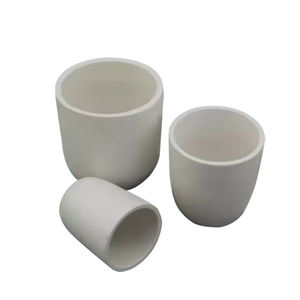
2. Processing and Microstructural Engineering
( Silicon Carbide Ceramics)
2.1 Sintering and Densification Techniques
Silicon carbide is inherently tough to compress as a result of its solid covalent bonding and reduced self-diffusion coefficients, needing innovative handling techniques to achieve full density without ingredients or with very little sintering aids.
Pressureless sintering of submicron SiC powders is possible with the addition of boron and carbon, which promote densification by removing oxide layers and enhancing solid-state diffusion.
Hot pressing applies uniaxial pressure during home heating, making it possible for full densification at lower temperatures (~ 1800– 2000 ° C )and generating fine-grained, high-strength parts suitable for reducing devices and wear parts.
For big or complex forms, reaction bonding is utilized, where permeable carbon preforms are penetrated with molten silicon at ~ 1600 ° C, creating β-SiC in situ with minimal shrinking.
Nevertheless, recurring cost-free silicon (~ 5– 10%) continues to be in the microstructure, restricting high-temperature efficiency and oxidation resistance over 1300 ° C.
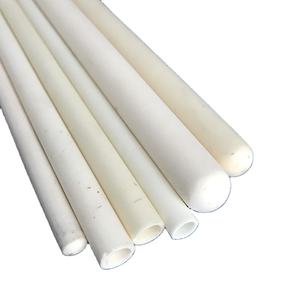
2.2 Additive Production and Near-Net-Shape Fabrication
Recent advancements in additive manufacturing (AM), especially binder jetting and stereolithography using SiC powders or preceramic polymers, enable the manufacture of complicated geometries previously unattainable with standard methods.
In polymer-derived ceramic (PDC) paths, liquid SiC precursors are formed using 3D printing and afterwards pyrolyzed at high temperatures to generate amorphous or nanocrystalline SiC, commonly needing additional densification.
These strategies reduce machining expenses and product waste, making SiC more easily accessible for aerospace, nuclear, and warm exchanger applications where complex layouts improve performance.
Post-processing actions such as chemical vapor infiltration (CVI) or liquid silicon seepage (LSI) are sometimes utilized to improve density and mechanical stability.
3. Mechanical, Thermal, and Environmental Efficiency
3.1 Toughness, Hardness, and Use Resistance
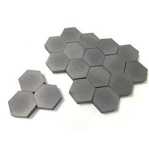
Silicon carbide places among the hardest known materials, with a Mohs firmness of ~ 9.5 and Vickers firmness exceeding 25 Grade point average, making it very immune to abrasion, erosion, and damaging.
Its flexural stamina generally ranges from 300 to 600 MPa, relying on processing technique and grain dimension, and it preserves toughness at temperature levels as much as 1400 ° C in inert environments.
Fracture durability, while modest (~ 3– 4 MPa · m ¹/ TWO), suffices for several architectural applications, specifically when combined with fiber reinforcement in ceramic matrix compounds (CMCs).
SiC-based CMCs are utilized in generator blades, combustor linings, and brake systems, where they supply weight cost savings, gas effectiveness, and extended service life over metal equivalents.
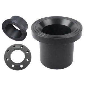
Its excellent wear resistance makes SiC perfect for seals, bearings, pump elements, and ballistic shield, where longevity under severe mechanical loading is crucial.
3.2 Thermal Conductivity and Oxidation Security
One of SiC’s most beneficial residential properties is its high thermal conductivity– as much as 490 W/m · K for single-crystal 4H-SiC and ~ 30– 120 W/m · K for polycrystalline kinds– surpassing that of several steels and allowing reliable warmth dissipation.
This property is critical in power electronic devices, where SiC tools create less waste warmth and can operate at higher power thickness than silicon-based gadgets.
At elevated temperature levels in oxidizing atmospheres, SiC creates a protective silica (SiO ₂) layer that slows down more oxidation, providing good ecological durability as much as ~ 1600 ° C.
However, in water vapor-rich settings, this layer can volatilize as Si(OH)₄, bring about sped up degradation– a vital challenge in gas generator applications.
4. Advanced Applications in Power, Electronics, and Aerospace
4.1 Power Electronic Devices and Semiconductor Gadgets
Silicon carbide has actually transformed power electronics by making it possible for gadgets such as Schottky diodes, MOSFETs, and JFETs that operate at greater voltages, frequencies, and temperatures than silicon equivalents.
These devices reduce energy losses in electric vehicles, renewable energy inverters, and industrial motor drives, adding to international power effectiveness enhancements.
The ability to operate at junction temperatures above 200 ° C permits simplified cooling systems and increased system dependability.
Furthermore, SiC wafers are utilized as substrates for gallium nitride (GaN) epitaxy in high-electron-mobility transistors (HEMTs), combining the benefits of both wide-bandgap semiconductors.
4.2 Nuclear, Aerospace, and Optical Solutions
In nuclear reactors, SiC is a key component of accident-tolerant gas cladding, where its low neutron absorption cross-section, radiation resistance, and high-temperature toughness boost safety and security and performance.
In aerospace, SiC fiber-reinforced compounds are utilized in jet engines and hypersonic lorries for their lightweight and thermal stability.
In addition, ultra-smooth SiC mirrors are used precede telescopes because of their high stiffness-to-density proportion, thermal stability, and polishability to sub-nanometer roughness.
In summary, silicon carbide ceramics stand for a cornerstone of modern-day sophisticated materials, incorporating extraordinary mechanical, thermal, and digital properties.
With precise control of polytype, microstructure, and processing, SiC continues to make it possible for technological advancements in power, transportation, and extreme environment engineering.
5. Distributor
TRUNNANO is a supplier of Spherical Tungsten Powder with over 12 years of experience in nano-building energy conservation and nanotechnology development. It accepts payment via Credit Card, T/T, West Union and Paypal. Trunnano will ship the goods to customers overseas through FedEx, DHL, by air, or by sea. If you want to know more about Spherical Tungsten Powder, please feel free to contact us and send an inquiry(sales5@nanotrun.com).
Tags: silicon carbide ceramic,silicon carbide ceramic products, industry ceramic
All articles and pictures are from the Internet. If there are any copyright issues, please contact us in time to delete.
Inquiry us


